
| Contents |
| Dragon HW |
| Dragon SW (DDOS) |
| Dragon SW (OS9) |
| Dragon Projects |
Dragon OS9 Real Time Clock
This projects creates a Real Time Clock (RTC) for use with the Dragon under OS9. To start with you must have some kind of IO expandability not available on an unmodified Dragon - additional address decode logic which provides 1 free 4 byte slot in the IO map. Details of address decoding and IO expansion are covered in the address decode section of my web page. During this article, the signal name AD is used to denote the output of the address decoder.
RTC Hardware
The Real Time clock chip utilised is a Hitachi 146818 device which is also used by PC's. The chip itself provides 64 bytes of information comprising 14 bytes dedicated to control of the RTC and 50 bytes of free CMOS RAM. On the PC, this is used to hold the BIOS settings. As it is mapped on the PC, the chip appears as a contiguous block of memory. In the Dragon design, it will be encoded to fit into 2 bytes due to lack of IO space in the memory map. One byte will be used as an address register which when written to with a value between 0-63 will determine the memory location within the chip that the next read/write of the data register (the other byte) will access.
RTC Pinout

Pin#    Name    Description

  1     N.C.    Not Connected
  2     OSC1    Clock In 1
  3     OSC2    Clock In 2
 4-11   AD0-AD7 Address/Data Lines
 12     VSS     0V
 13     CE~     Chip Enable
 14     AS      Address Strobe
 15     R/W~    Read/Write enable
 16     N.C.    Not Connected
 17     DS      Data Strobe
 18     RESET~  Chip Reset
 19     IRQ~    Interrupt output
 20     CK O/P  Clock Output Select
 21     CK O/P  Clock Output
 22     PWR SNS Power Sense
 23     SQR OP  Square wave output
 24     VCC     +5V
The connections to the Dragon are shown below. Pins not identified are not used in the circuit.
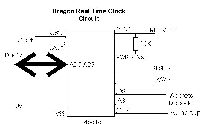
The circuit design is essentially broken down into 3 sections:
- address decode, for interfacing to the Dragon's address & data bus.
- clock circuit, crystal and clocking for the chip
- psu holdup, battery backup circuitry for keeping time when the machine is switched off.
1. Clock circuit.
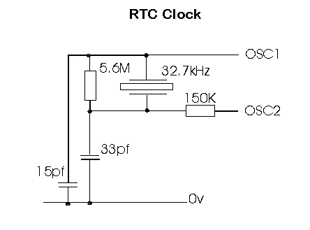
This connects to the chip via the OSC1 & 2 pins and consists of a standard crystal circuit using a 32.768khz crystal. The chip may also be clocked at 4.194Mhz or 1.0485Mhz but the lower speed version consumes less power when the chip is in standby mode running off the battery.
2. Address decode.
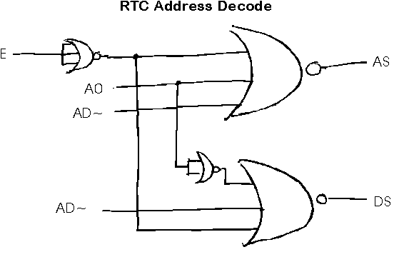
The data lines of the RTC connect directly to the Dragon's CPU data lines, as does R/W and RESET. The address decode logic consists of 4 NOR gates, 3 of them being of the 3 input variety. Thus the address decode circuitry is contained on two logic chips.
The principal decode inputs to the chip are AS and DS (both active high). For the data lines to be treated as an address to the chip (0-63 locations) AS has to be asserted, and for data lines DS has to be asserted.
For the Dragon circuit, AS needs to be asserted when the chip is selected, and the first byte of the IO region is selected. So, by NORing together AD (from the address decode circuit) and A0 a logic 1 will be gained if both are low. Add to that the inverted E clock (6809 data bus is only valid when E is high) and the AS decode is complete.
The DS decode is almost identical, except the A0 signal is inverted - so it is only activated when the 2nd byte in the IO region is activated.
Whilst the circuit works, it is rather sloppy as Chip Enable (CE~) is not used at all during the address decoder, instead it is permanently selected by the PSU holdup circuit. This means there is a slight chance of erroneous data being written into the chip when the machine is powered down and the lines go into an undefined state. Unfortunatly, CE~ cannot be tied easily into the main decode circuit, as it would go inactive between each chip access. The RTC must be accessed as follows:
        Assert CE~
        Assert AS and write address to chip
        Assert DS and read/write data to chip
        De-assert CE~
As the 6809 cannot perform this in one cycle, the effect of CE~ dropping between performing the AS access and the DS access would be the chip resetting and expecting another AS access. So, for simplicity CE~ is effectively permanently selected.
3. PSU Holdup
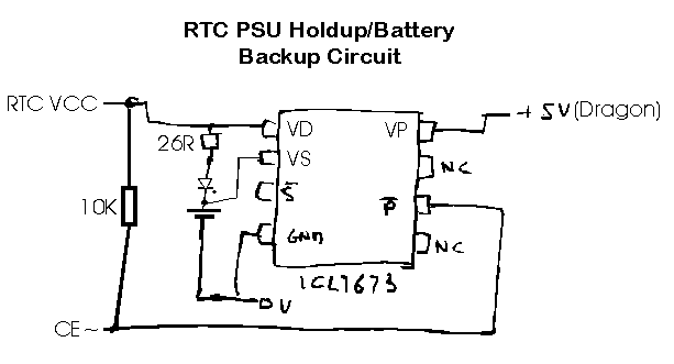
The RTC needs to remain powered even when the Dragon is switched off to maintain the current date/time so a simple PSU holdup circuit is used to achieve this. A dedicated battery backup chip (ICL7673) is used which takes as input a 5V battery and the Dragon's main 5V rail and provides an uninterrupted 5V rail to the RTC clock. This output should be used to drive the 5V rail of the RTC, not the standard Dragon's 5V rail. The chip detects a power drop on the main power rail and switches over to the battery automatically. In addition, it also releases the CE~ line to prevent the chip being erroneously accessed.
When the Dragon is powered, the chip can trickle charge the battery to prevent it discharging over time. If recharging of the battery is not required, the 26R resistor and diode part of the circuit can be omitted.
Parts List
----------

 1 * 146818 Real Time Clock + Data Sheet
 1 * ICL7673 Battery Backup IC
 1 * 74LS(HC)02 2 input NOR gates
 1 * 74LS(HC)27 3 input NOR gates
 2 * 10K resistors
 1 * 150K
 1 * 5.6M
 1 * 26R
 1 * 32.7khz crystal
 1 * 33pf cap
 1 * 15pf cap
 1 * 1N4001 Diode
 1 * 3-5V battery
The choice of battery is down to you - if a non-rechargeable battery is used then the trickle charge part of the circuit MUST be removed. Maplin stock 3.6V PCB mounting batteries which may be deemed ideal for this task. I have used 3 standard AA Ni-Cads in a pack wedged underneath the keyboard.
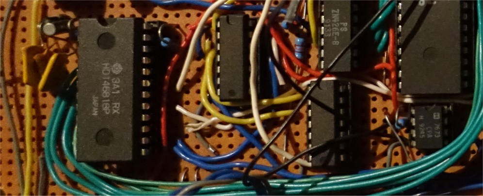
The RTC is the large chip on the left of the photo whilst the ICL7673
hold up is the small 8-pin device sat underneath the PIA on the right
hand side. Finally the logic gates are the two devices which appear to
have no writing on them..
RTC Software
As mentioned previously, the interface to the Dragon consists of two bytes: an address location and data location. Therefore, access to the chip involves two chip accesses - the address followed by data access. This _must_ always occur, even if the same data location is to be accessed twice in a row.
The key parts of the address map are:
 Addr   Description

  0     Seconds
  1     Seconds Alarm
  2     Minutes
  3     Minutes Alarm
  4     Hours (12 or 24 selectable)
  5     Hours Alarm (12 or 24 selectable)
  6     Day of week (Sunday=1)
  7     Day of month
  8     Month
  9     Year
 10     Register 'A'
 11     Register 'B'
 12     Register 'C'
 13     Register 'D'
 14-63  Free CMOS RAM
The CMOS RAM is not particularly useful on the Dragon - it can be accessed freely if required though.
For the purposes of this example, I will assume the chip is mapped at $FF18:FF19 on the Dragon.
Therefore, if I wanted to write $FF to location 50 in the CMOS RAM:
        lda #50      address locn
        sta $ff18
        lda #$ff     data byte
        sta $ff19
In principal, programming the chip is that straightforward: the time of day is written into the correct locations on the chip and it can be read back when required. Likewise, an alarm time can also be programmed which can be detected in software through one of the 4 miscellaneous control registers.
Example: Thur 8th May 1997, 10:50:23
        clrb
        stb $ff18       Addr locn. 0
        lda #23         seconds
        sta $ff19       into seconds register
        addb #2
        stb $ff18       Addr locn. 2
        lda #50
        sta $ff19       into minutes register

        ...
The time of day can be read in a similar fashion:
        clrb
        stb $ff18
        lda $ff19       A = seconds value
As always, things aren't quite that straightforward. Before the chip can be programmed, some initilisation needs to be performed. This essentially involves programming the clock divide rate and 12/24 hour mode setting - performed through register A & B:
        lda #10         Reg A address
        sta $ff18
        lda #32         set for 32.768khz crystal
        sta $ff19
        lda #11         Reg B address
        sta $ff18
        lda #6          set for standard binary mode, 24 hour clock
        sta $ff19
The register breakdown is fully explained in the chip's data sheet. As a footnote, bit 1 of register B is the 12/24 hour select, clearing it sets 12 hour mode.
This sets the chip up for normal use. However, before you access any of the RTC information you must ensure that the chip itself is not updating any registers. Each time the chip needs to update a register it should not be accessed for 1984us or invalid data is returned.
To detect this, the top bit of register A is used as an update in progress bit (UIP bit). Prior to accessing any registser, this bit should be tested for a 1. If it is set, the CPU should wait until it clears:
clcknr lda #10       load register A addr
       sta $ff18
       lda $ff19     load register a
       lsla          test for UIP
       bcs clcknr    clock in update, wait?

        ... proceed to access clock
Note: the CPU has 244us to perform whatever data transfers are necessary before the RTC may need to update itself. This should be sufficient time for the Dragon to read the date/time info successfully.
Finally, when the time is being entered into the chip, it is a good idea to reset the clock and abort/hold-off any chip updates which may occur.
This is achieved by writing a value of 96 to the A register to reset the clock and a value of 134 to the B registser. By setting the top bit of this register, no RTC updates will occur.
The chip is capable of much more than I have outlined here and the data sheet provides all of the information to make use of these facilities including setting and detecting the 24 hour alarm. For the Dragon design as it stands, the alarm can only be detected by software polling of register C - as we have not used the IRQ line of the chip it cannot generate an interrupt to the CPU. However, if this is desired you can connect this pin directly to the IRQ~ line of the 6809 without any problems.
Finally, I have included an assembler listing of a replacement Clock module for OS9. All that needs to change is the definitions of the RTC base address ClockAS and ClockDS to whereever your RTC is mapped. Then, create a new OS9 Boot disk from scratch using OS9Gen but removing the old clock module.
In order to start your clock module, include a 'setime' statement in your 'startup' file eg.
setime 97/1/1 0:0:0
The time parameters are ignored with this, it merely serves to install the clock into OS9.