
| Contents |
| Dragon HW |
| Dragon SW (DDOS) |
| Dragon SW (OS9) |
| Dragon Projects |
Alternative Decoder Mods
CPU Piggy Back
An alternative to the cartridge port decoder is to piggy back your extender board into the CPU socket (this I have tried recently and know that it works). By using a 40 pin DIL wire wrap socket (possibly firstly going into an ordinary 40 pin socket to stop it springing out of the Dragon's CPU socket, which it has a tendency to do) you should be able to remove the CPU from the machine and piggy back it onto a bit of strip board:
        -------------  CPU
        |           |          strip board
  --------------------------------------
        |           |
        |           |  40 Pin wire wrap
        |           |  socket
        |           |
        |           |
        -------------
        |           |  40 pin DIL skt
        -------------
        |           |  existing CPU skt
------------------------------------------
          Main Board
This arrangement should give you access to the Dragon's address and data bus. You may still need access to some pins on the cartridge port (eg. EXMEM or the P2 decoder lines). If the port is occupied you will have to resort to soldering wires to the relevent pins on the board. If the port isn't you can use a small piece of stripboard to get at a couple of pins - only if they are on one side of the edge connector though.
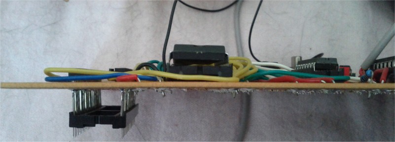
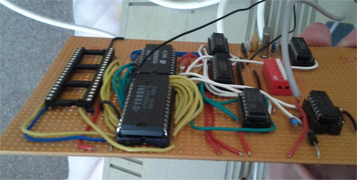
Above images show one of my Network Cards using this type of configuration
Quick Address Decoder
The 'clean' way decode an area of memory is outlined in the address decoding document written for Up2Date using the EXMEM line (brought out onto the cartridge port) to disable the internal decoding. However, a lot of people make use of the unused areas mapped to the SAM chip, which since it does not have access to the data bus, can be used quite easily for add on boards, particularly if you only want to add 1 or 2 devices. The area between $FFE0 and $FFF1 is one such 'reserved area'. So in order to map to this area, all you need is to use some logic chips to determine when an address in this range has been specified - in fact the decoder is essentially a cut down version of the fully blown variant.
The first thing to consider, is that the top 8 bits must all be set in order to get close to our memory area. By using an 8-input NAND get (74LS30) we can derive a single line which will go low when all the upper bits of the address bus are set:
              74LS30
  A15  -----|---------*
  A14  -----|         *
  A13  -----|         *
  A12  -----|         *0 ----->  low when address $FFxx is o/p
  A11  -----|         *            when xx = don't care
  A10  -----|         *
  A9   -----|         *
  A8   -----|---------*
Next, we need to decode for the range $E0 through to $F1:
 Address bit
  7 6 5 4 3 2 1 0
  1 1 1 0 x x x x    = $Ex
  1 1 1 1 x x x x    = $Fx
With a bit of trickiness, a 74LS138 3 to 8 decoder should suffice:
                        74LS138
O/P from 74LS30  ---->     E1~
             A4  ---->     E2~
            +5V  ---->     E3
             A5  ---->     A0
             A6  ---->     A1
             A7  ---->     A2
The 3-8 decoder takes in a 3 bit binary number (which gives 0(000) to 7(111)) and sets one of 8 outputs accordingly. The chip has 3 enable lines, 2 of which are active low (denoted by the ~ symbol). This means, to activate them, the line must go to 0V as opposed to +5V. The chip is only ever enabled, when the output from the 74LS30 is low ($FFxx), and A4 is also low (the third enable line is permanently set). Once the chip is in this configuration, the other 3 address lines we are interested in (A5,A6,A7) form the 3 inputs to the decoder. Since we are only interested in when all three are high giving a binary number of 7(111), output 7 from the decoder will give us an address in the range $FFE0 -> $FFEF which should suffice.